Make your own Solar Cells
types of cells
silicon PV cells
- monocrystaline - more expensive - more efficient
- polycrystaline - less expensive - less efficient
- Amorphous - even ess expensive, even less efficient.
Multi junction
taken from http://science.nasa.gov/science-news/science-at-nasa/2002/solarcells/
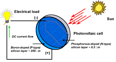
Today's most common PV devices use a single junction, or interface, to create an electric field within a semiconductor such as a PV cell. In a single-junction PV cell, only photons whose energy is equal to or greater than the band gap of the cell material can free an electron for an electric circuit. In other words, the photovoltaic response of single-junction cells is limited to the portion of the sun's spectrum whose energy is above the band gap of the absorbing material, and lower-energy photons are not used.
One way to get around this limitation is to use two (or more) different cells, with more than one band gap and more than one junction, to generate a voltage. These are referred to as "multijunction" cells (also called "cascade" or "tandem" cells). Multijunction devices can achieve a higher total conversion efficiency because they can convert more of the energy spectrum of light to electricity.
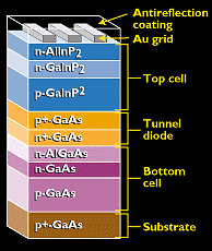
As shown below, a multijunction device is a stack of individual single-junction cells in descending order of band gap (Eg). The top cell captures the high-energy photons and passes the rest of the photons on to be absorbed by lower-band-gap cells.
Much of today's research in multijunction cells focuses on gallium arsenide as one (or all) of the component cells. Such cells have reached efficiencies of around 35% under concentrated sunlight. Other materials studied for multijunction devices have been amorphous silicon and copper indium diselenide. As an example, the multijunction device below uses a top cell of gallium indium phosphide, "a tunnel junction," to aid the flow of electrons between the cells, and a bottom cell of gallium arsenide.
how do they work
How are they made
What is required
silicon
- vacuum chamber
- silicon substrate
- a method if doping
- a method deposition
- phosphorus diffusion furnace
- a method of curing
- coating
patent search
Further reading
- http://search.nrel.gov/query.html?qp=&style=eere&qs=&qc=eren&ws=0&qm=0&st=1&nh=10&lk=1&rf=0&oq=&col=eren&qt=Multi-junction+solar+cells&x=0&y=0
- http://techportal.eere.energy.gov/category.do/categoryID=15
- Staebler-Wronski Effect
- junctions
- gallium arsenide (GaAs(
- InP ??
- processes
- Epitaxial liftoff technology
- Wafer bonding

